SHAPING THE FUTURE OF GREEN NANOTECHNOLOGY
We work with van der Waals materials known as transition metal dichalcogenides (TMDs). TMDs are an emerging class of materials for new research frontiers and future applications.
Nanopatterning can change TMD properties in a structure-dependent manner. Our service is to fabricate and deliver such structures.
OUR PRODUCTSPRODUCTS
OUR SERVICE IS BASED ON A LONG-TERM EXPERIENCE OF WORKING WITH TMDs AND NANOFABRICATION.
- Unique nanostructured TMDs.
- Atomically sharp edges.
- Custom designs to fit your application.
NANOSTRUCTURED TMDs
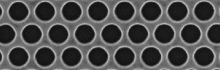
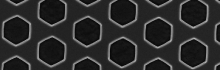
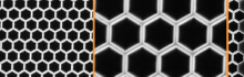
STANDARD HEXAGONAL HOLE ARRAY
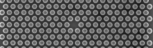
STANDARD HEXAGONAL DISK ARRAY
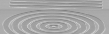
STANDARD TMD GRATING
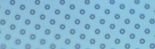
NANOSTRUCTURED MoS2
ATOMICALLY SHARP HOLES IN MoS2
NANOSTRUCTURED WS2
ATOMICALLY SHARP HOLES IN WS2
TMD NANOCRYSTALS
STAND-ALONE NANO-PATTERNED TMD CRYSTALS
APPLICATIONS
MATERIAL FEATURES & APPLICATIONS FOR INDUSTRY
Molybdenum disulfide (MoS2) and tungsten disulfide (WS2) are semiconducting analogs of famous graphene. Especially MoS2 is used in industry already now, as a catalyst for oil desulfurization reaction and as a lubricant additive.
We discovered a way to significantly improve the properties of natural MoS2 by introducing perfect and highly controllable edges in the material.
ELECTRONICS
Zigzag edges that we create are ferromagnetic and metallic, unlike semiconducting planes.
SENSORS
Exposed edges allow to improve the sensitivity of sensors.
SCALABILITY
The material can be prepared in large quantities and in different forms, including colloidal solutions, sprays, and powders.
CATALYSIS
Our method allows us to significantly improve catalytic activity by exposing relevant zigzag edges in massive amounts.
MECHANICS
TMDs are highly bendable and mechanically strong.
OPTICS
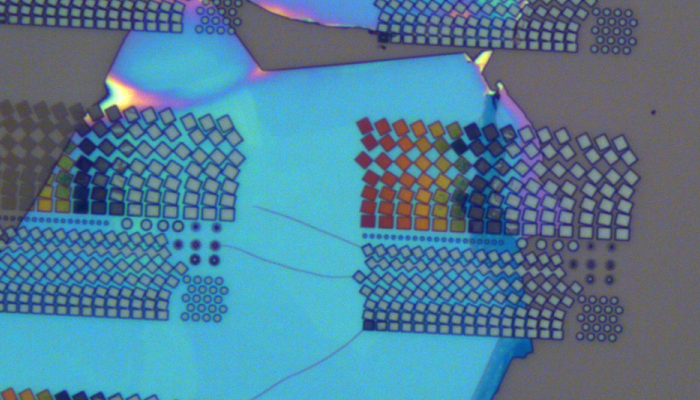
The color of the reflected or transmitted light can be controlled across the entire visible range – from blue to red.
ABOUT PRODUCTION
OPTICAL MICROSCOPY IMAGES
Nanostructured TMDs support vivid colors across the whole visible spectrum and beyond. An example of true-color optical images of nanopatterned TMD is shown here.
Publications
We have a long-term experience working with TMDs and their nanopatterning. Our work is based on several high-profile scientific publications, including:
As well as a number of on-going activities in our Research Group.
OUR RESEARCH GROUP